Contents of the invention
The invention proposes a micro-LED dead pixel detection method, system, equipment and medium, aiming at solving the technical problem of how to improve the efficiency of micro-LED dead pixel detection.
In this embodiment, the dead pixel detection method of described micro-LED comprises:
an automatic optical detection is carried out on the micro-LED on the wafer to obtain an automatic optical detection result, and a photoluminescence detection is carried out on the micro-LED on the wafer to obtain a photoluminescence detection result;
determining a set of suspected points, a set of good points and a set of first bad points according to the automatic optical detection result and the photoluminescence detection result;
electroluminescence detection is carried out on each micro-LED in the suspected point set and the good point set to obtain a second bad pixel set;
the union of the first set of dead pixels and the second set of dead pixels as the result of the detection of dead pixels.
Optionally, the steps for determining a set of suspected points, a set of good points, and a set of first bad points according to the automatic optical detection result and the photoluminescence detection result comprises:
based on the intersection of the good points in the automatic optical detection result and the good points in the photoluminescence detection result, a set of good points is obtained;
the first set of dead pixels is obtained based on the union of the dead pixels in the automatic optical detection result and the dead pixels in the photoluminescence detection result;
a set of suspicious points is obtained by taking a point on the wafer that does not belong to the set of good points and does not belong to the first set of bad points as a suspicious point.
Optionally, after determining a set of suspected points, a set of good points and a set of first bad points according to the automatic optical detection result and the photoluminescence detection result, the method further comprises:
randomly selecting the good points in the set of good points to obtain a set of random good points;
the steps of electroluminescence detection of each micro-LED in the suspected point set and the good point set to obtain a second bad pixel set, comprising:
electroluminescence detection is carried out on each micro-LED in the suspected point set and the random good point set to obtain a second bad pixel set.
Optionally, the steps for electroluminescence detection of each micro-LED in the suspect point set and the random good point set to obtain a second bad pixel set comprises:
obtaining the coordinates corresponding to each micro-LED in the suspected point set and the random good point set, and determining the shortest path based on each coordinate;
electroluminescence detection is carried out on each micro-LED in the suspected point set and the random good point set according to the shortest path to obtain a second bad pixel set.
Optionally, after determining the steps of the shortest path based on each of the coordinates, the method further comprises:
optimizing the shortest path based on the preset trajectory planning principle;
The steps of electroluminescence detection of each micro-LED in the suspect point set and the good point set according to the shortest path to obtain a second bad pixel set, comprising:
electroluminescence detection is carried out on each micro-LED in the suspected point set and the good point set according to the shortest path after optimization, and a second bad pixel set is obtained.
Optionally, after performing electroluminescence detection on each micro-LED in the suspected point set and the good point set to obtain a second bad pixel set, the method further comprises:
determining the intersection of the set of good points and the set of second bad points, and determining the first quantity of micro-LEDs in the intersection;
determine the second quantity of micro-LEDs in the set of good spots, and take the ratio of the first quantity to the second quantity as the bad pixel detection rate.
Optionally, the method further comprises, prior to the steps of performing an automated optical inspection of a micro-LED on a wafer to obtain an automated optical inspection result:
The preset motion table is controlled to perform raster scanning motion through an iterative learning algorithm, wherein the wafer is fixed on the motion table.
In addition, in order to solve the above problem, the invention also provides a dead pixel detection system of micro-LED, and the dead pixel detection system of micro-LED comprises:
the scanning detection module is used for carrying out automatic optical detection on the micro-LED on the wafer to obtain the automatic optical detection result, and performing photoluminescence detection on the micro-LED on the wafer to obtain the photoluminescence detection result;
the luminescent spot classification module is used for determining a set of suspected points, a set of good points and a set of first bad points according to the automatic optical detection result and the photoluminescence detection result;
the electroluminescence detection module is used for electroluminescence detection of each micro-LED in the suspected point set and the good point set to obtain a second bad point set;
the bad pixel aggregation module is used for taking the union of the first bad pixel set and the second bad pixel set as the bad pixel detection result.
In addition, in order to solve the problem, the invention also provides a dead pixel detection device of micro-LED, the dead pixel detection device of micro-LED comprises: memory, a processor and a dead pixel detection program of micro-LED stored on described memory and can run on described processor, and the dead pixel detection program of described micro-LED is executed by described processor when the bad pixel detection method of micro-LED is executed as described above.
In addition, in order to solve the problem, the invention also provides a storage medium, the storage medium is stored with a dead pixel detection program of micro-LED, and the dead pixel detection program of micro-LED is executed by a processor to realize the steps of the dead pixel detection method of micro-LED as described above.
In the embodiment of the present invention, an automatic optical detection result is obtained by performing an automatic optical detection on a micro-LED on a wafer, and a photoluminescence detection result is carried out on a micro-LED on the wafer to obtain a photoluminescence detection result, and the micro-LED on the wafer can be rapidly detected by automatic optical detection and photoluminescence detection; then determine a set of suspected points, a set of good points and a set of first bad pixels according to the results of the automatic optical detection and the photoluminescence detection results, and preliminarily screen out the bad pixels according to the results of the rapid detection; then electroluminescence detection is carried out on each micro-LED in the suspect point set and the good point set to obtain a second bad pixel set, which can be further detected for the suspected point and the good point, so that the bad pixel can be accurately detected on the basis of reducing the detection time; then the union of the first bad pixel set and the second bad pixel set is taken as the bad pixel detection result to obtain the dead pixel set on the wafer.
The present invention screens out the first bad pixel set through a rapid detection result, can determine part of the bad pixel in a relatively short time, and then carries out electroluminescence detection on the good spot set and the suspected point set, not only can reduce the overall time consumption of electroluminescence detection, but also can take into account the accuracy of micro-LED detection, thereby realizing the effect of taking into account the bad pixel detection speed and the bad pixel detection accuracy, thereby achieving the purpose of improving the efficiency of micro-LED bad pixel detection.
The specific embodiment
It should be understood that the specific embodiments described herein are only used to explain the present invention and are not intended to qualify the invention.
The technical solutions in the embodiments of the present invention will be clearly and completely described below in conjunction with the accompanying drawings in the embodiments of the present invention, and it is obvious that the described embodiments are only part of the embodiments of the present invention, not all embodiments. Based on the embodiments in the present invention, all other embodiments obtained by a person skilled in the art without making creative labor belong to the scope of protection of the present invention.
It should be noted that all directional indications (such as up, down, left, right, front, rear, ......) in the embodiment of the present invention It is only used to explain the relative position relationship between the parts and the movement of each part in a specific posture (as shown in the attached drawing), and if the specific attitude changes, the directional indication will change accordingly.
In the present invention, unless otherwise expressly specified or qualified, the terms "connected", "fixed", etc., shall be construed broadly, for example, "fixed" may be a fixed connection, a detachable connection, or a whole; It can be mechanically or electrically connected; It can be directly connected or indirectly connected by an intermediate medium, it may be an internal connection between two elements or an interaction between two elements, unless otherwise expressly specified. For a person of ordinary skill in the art, the specific meaning of the above terms in the present invention may be understood according to the specific circumstances.
In addition, descriptions such as "first", "second", etc., in the present invention are for descriptive purposes only and cannot be construed as indicating or implying their relative importance or implying the number of technical features indicated. Thus, defining the "first" and "second" features may explicitly or implicitly include at least one of those features. In addition, the technical solutions between the various embodiments may be combined with each other, but they must be based on those who are skilled in the art and can be realized, and when the combination of technical solutions is contradictory or impossible to realize, it shall be deemed that the combination of such technical solutions does not exist and is not within the scope of protection claimed by the present invention.
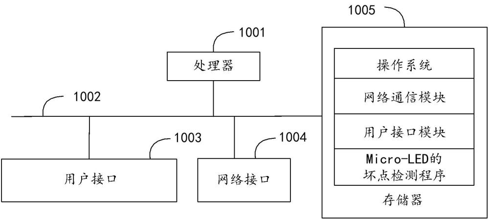
As shown in FIG. 1, FIG. 1 is a schematic diagram of the equipment structure of the hardware operating environment of the hardware operating environment of the micro-LED dead pixel detection equipment involved in the embodiment scheme of the present invention.
As shown in Figure 1, in the hardware operating environment of the micro-LED dead pixel detection device, the micro-LED dead pixel detection device may include: a processor 1001, such as a CPU, a network interface 1004, a user interface 1003, a memory 1005, and a communication bus 1002. wherein, the communication bus 1002 is used to realize the connection communication between these components. The user interface 1003 can include a display screen (Display), an input unit such as a keyboard (Keyboard), and the optional user interface 1003 can also include a standard wired interface and a wireless interface. NETWORK INTERFACE 1004 CAN OPTIONALLY INCLUDE STANDARD WIRED INTERFACES AND WIRELESS INTERFACES (SUCH AS WI-FI INTERFACES). Memory 1005 can be either high-speed RAM memory or non-volatile memory, such as disk memory. Memory 1005 may also be an optional storage device independent of the aforementioned processor 1001.
Those skilled in the art can understand that the structure of the micro-LED dead pixel detection equipment shown in Figure 1 does not constitute a limitation of the micro-LED dead pixel detection equipment, and may include more or fewer parts than illustrated, or combine certain parts, or arrange different parts.
As shown in Figure 1, memory 1005, which is a computer storage medium, may include an operating system, a network communication module, a user interface module, and a micro-LED dead pixel detection program.
In the device shown in Figure 1, the network interface 1004 is mainly used to connect to the background server and carry out data communication with the background server; The user interface 1003 is mainly used for connecting the client (user terminal) and carrying out data communication with the client; The processor 1001 can be used to invoke the dead pixel detection program of the micro-LED stored in memory 1005 and perform the following operations:
an automatic optical detection is carried out on the micro-LED on the wafer to obtain an automatic optical detection result, and a photoluminescence detection is carried out on the micro-LED on the wafer to obtain a photoluminescence detection result;
determining a set of suspected points, a set of good points and a set of first bad points according to the automatic optical detection result and the photoluminescence detection result;
electroluminescence detection is carried out on each micro-LED in the suspected point set and the good point set to obtain a second bad pixel set;
the union of the first set of dead pixels and the second set of dead pixels as the result of the detection of dead pixels.
Based on the above-mentioned hardware structure, the overall conception of each embodiment of the dead pixel detection method of micro-LED of the present invention is proposed.
Nowadays, micro-LED inspection can be divided into non-contact inspection and contact detection. Among them, the non-contact detection speed is fast, but the detection accuracy is low; The contact detection accuracy is high, but the detection speed is slow. On the one hand, although non-contact detection can meet the demand for speed, due to the low accuracy, it may lead to missed detection or false detection, which affects the quality of micro-LED dead pixel detection. On the other hand, contact detection, although highly accurate, is slow to detect, thus limiting its application on high-speed production lines.
Therefore, how to improve the efficiency of micro-LED dead pixel detection is a technical problem that has yet to be solved by those skilled in the art.
In order to solve the above problem, the invention proposes a dead pixel detection method of micro-LED.
Based on the overall conception of each embodiment of the dead pixel detection method of micro-LED of the present invention, each embodiment of the dead pixel detection method of micro-LED of the present invention is proposed.
It should be noted that the execution body of the dead pixel detection method of the present invention micro-LED is the bad pixel detection equipment of micro-LED, and the equipment can be a computer, a server and other terminal equipment. For ease of explanation, in the following embodiments, the executive body is omitted for elaboration.
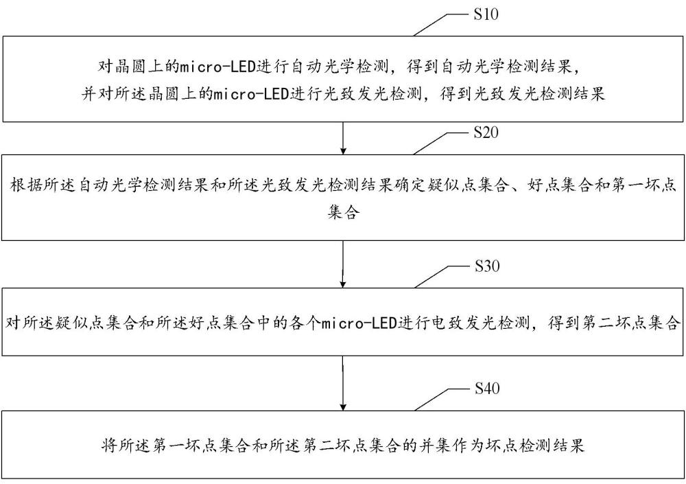
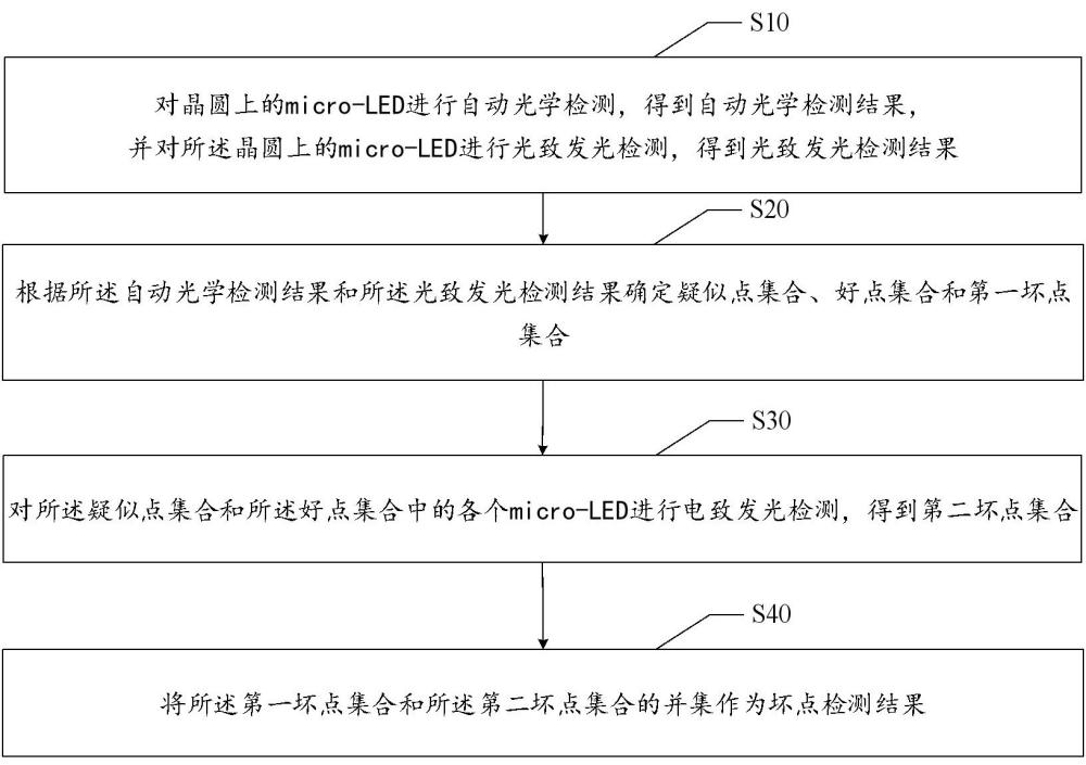
Please refer to Figure 2, and Figure 2 is a schematic diagram of the flow of the first embodiment of the dead pixel detection method of micro-LED of the present invention. It should be noted that, although the logical order is shown in the flow diagram, in some cases, of course, the individual steps of the dead pixel detection method of the present invention micro-LED can be executed in a different order than here.
In this embodiment, the dead pixel detection method of described micro-LED comprises:
step S10, perform an automatic optical detection on the micro-LED on the wafer to obtain an automatic optical detection result, and perform a photoluminescence detection on the micro-LED on the wafer to obtain a photoluminescence detection result;
It should be noted that micro-LED on the wafer refers to the light-emitting point on the wafer, automatic optical inspection refers to AOI detection, and photoluminescence inspection refers to PL detection.
In this embodiment, when performing automatic optical detection of micro-LED on a wafer, the luminescence image of the micro-LED can be collected through an image sensor, and then the luminescence image is processed by machine learning, big data analysis, etc., so that an automatic optical detection result can be obtained; When photoluminescence detection is performed on micro-LEDs on wafers, luminescence information can be obtained through spectrometers, photometers, and colorimeters, so that photoluminescence results can be obtained based on luminous intensity, chromaticity, and brightness information in the luminescence information.
It should be noted that the present invention does not limit the realization mode of automatic optical detection and photoluminescence detection.
step S20, determining a set of suspected points, a set of good points and a set of first bad points according to the automatic optical detection result and the photoluminescence detection result;
It should be noted that the collection of suspicious points refers to the set composed of suspicious points, and the suspicious points refer to the luminous points that are suspected of not emitting light. A good spot is a collection of luminous points that can emit light normally, and a set of good dots is a collection of luminous dots that emit light normally. A bad pixel is a collection of luminous dots that cannot emit light, and a set of dead pixels is a collection of luminous dots that cannot emit light.
In the present embodiment, the automated optical detection result comprises a suspicious, good, and bad pixel detected by automated optics, and the photoluminescence detection result also comprises a suspicious, good, and bad pixel detected by photoluminescence. Therefore, the good points detected by automatic optics and the good points detected by photoluminescence can be sorted out to obtain a set of good points, and the suspicious points detected by automatic optics and the suspected points detected by photoluminescence can be sorted out to obtain a collection of suspected points, and the bad pixels detected by automatic optics and the bad points detected by photoluminescence can be sorted out to obtain the first set of bad pixels.
As an example, the union of good points detected by automated optics and good points detected by photoluminescence can be used as a good point set.
Optionally, in a feasible embodiment, the preceding step S20 further comprises:
step S201, obtaining a set of good points based on the intersection of the good points in the automatic optical detection result and the good points in the photoluminescence detection results;
step S202, obtaining a first set of dead pixels based on the union of the dead pixels in the automatic optical detection result and the dead pixels in the photoluminescence detection result;
step S203, a point on the wafer that does not belong to the set of good points and does not belong to the first set of bad points is taken as a suspicious point to obtain a set of suspicious points.
As an example, in order to improve the accuracy of dead pixel detection, the intersection of the good pixels in the AE detection results and the good pixels in the photoluminescence detection results can also be used as a set of good pixels, and the union of the bad pixels in the AE results and the bad pixels in the photoluminescence detection results can be used as the first bad pixel set. Then, the points on the wafer that belong to neither the good point set nor the first bad point set are taken as the suspicious points, and then multiple suspicious points are summarized to obtain the suspicious point set.
step S30, electroluminescence detection is carried out on each micro-LED in the suspected point set and the good point set to obtain a second bad pixel set;
In this embodiment, after obtaining a set of suspected points and a set of good points, an electroluminescence detection can also be performed on each micro-LED in the set of suspected points and a set of good points, so as to obtain a second set of bad points.
As an example, luminescent point 1 is a luminous point in the suspected set of points, and if luminescent point 1 is detected in electroluminescence detection, if it is detected that luminous point 1 cannot emit light, then luminescent point 1 is a bad dot. After the luminous dots in the collection of suspicious and good dots are detected, all the bad pixels can be aggregated into a second set of bad pixels.
step S40, the union of the first set of bad pixels and the second set of bad pixels is taken as the result of the detection of bad pixels.
In this embodiment, after obtaining a first set of dead pixels and a set of second bad pixels, the union of the first set of dead pixels and the set of second dead pixels can be used as the result of bad pixel detection.
In this embodiment, an automatic optical detection result is obtained by performing an automatic optical detection on a micro-LED on a wafer, and a photoluminescence detection result is performed on a micro-LED on the wafer to obtain a photoluminescence detection result, and the micro-LED on the wafer can be rapidly detected by automatic optical detection and photoluminescence detection; then determine a set of suspected points, a set of good points and a set of first bad pixels according to the results of the automatic optical detection and the photoluminescence detection results, and preliminarily screen out the bad pixels according to the results of the rapid detection; then electroluminescence detection is carried out on each micro-LED in the suspect point set and the good point set to obtain a second bad pixel set, which can be further detected for the suspected point and the good point, so that the bad pixel can be accurately detected on the basis of reducing the detection time; then the union of the first bad pixel set and the second bad pixel set is taken as the bad pixel detection result to obtain the dead pixel set on the wafer.
The present invention screens out the first bad pixel set through a rapid detection result, can determine part of the bad pixel in a relatively short time, and then carries out electroluminescence detection on the good spot set and the suspected point set, not only can reduce the overall time consumption of electroluminescence detection, but also can take into account the accuracy of micro-LED detection, thereby realizing the effect of taking into account the bad pixel detection speed and the bad pixel detection accuracy, thereby achieving the purpose of improving the efficiency of micro-LED bad pixel detection.
Further, based on the first embodiment of the dead pixel detection method of micro-LED of the present invention, a second embodiment of the dead pixel detection method of micro-LED of the present invention is proposed.
In this embodiment, after the above step S20, the method further comprises:
step S100, randomly select the good points in the set of good points to obtain a set of random good points;
It should be noted that the random set of good points refers to the set of good points that are extracted.
In the present embodiment, after obtaining a set of good points, a part of the good points in the set of good points can also be randomly selected so as to facilitate the verification of the good points. That is, the extracted good points are detected twice by electroluminescence detection to judge the accuracy of automatic optical detection and photoluminescence detection.
Based on this, the above step S30 further comprises:
step S301, each micro-LED in the suspected point set and the random good point set are electroluminescently detected to obtain a second bad point set.
In a feasible embodiment, electroluminescence detection can also be performed on each micro-LED in the suspected point set and the random good point set, so as to obtain a second bad pixel set.
In the present embodiment, the invention can further reduce the number of luminescent spots to be detected during electroluminescence detection by extracting some good points for electroluminescence detection, so that the overall required time for bad pixel detection can be further reduced.
Optionally, in a feasible embodiment, the preceding step S301 further comprises:
step S3011, obtaining the coordinates corresponding to each micro-LED in the suspected point set and the random good point set, and determining the shortest path based on each coordinate;
step S3012, electroluminescence detection is carried out on each micro-LED in the suspected point set and the random good point set according to the shortest path to obtain a second bad pixel set.
It should be noted that the coordinates of each micro-LED on the wafer need to be determined when performing automatic optical inspection of micro-LEDs on wafers as well as photoluminescence inspection. For example, it is possible to set the coordinates of the micro-LEDs in the upper left corner of the wafer to (1,1) and then number the coordinates of the other micro-LEDs according to the matrix numbering scheme.
In the present embodiment, the coordinates of each micro-LED in the suspected point set and the random good point set can also be obtained, and then the shortest path between the coordinates is determined based on algorithms such as Dijkstra algorithm and Floyd algorithm. Then, according to the shortest path, electroluminescence detection is carried out on each suspected point and good point on the shortest path in turn, so that each suspected point and the bad point in the good point can be further determined. The dead pixels detected by electroluminescence detection can then be summarized to obtain a second set of dead pixels.
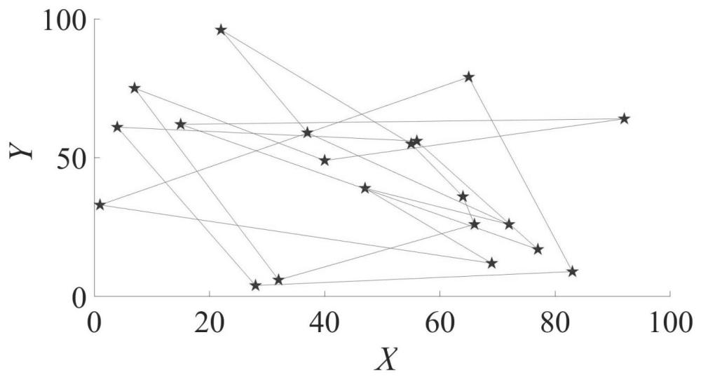
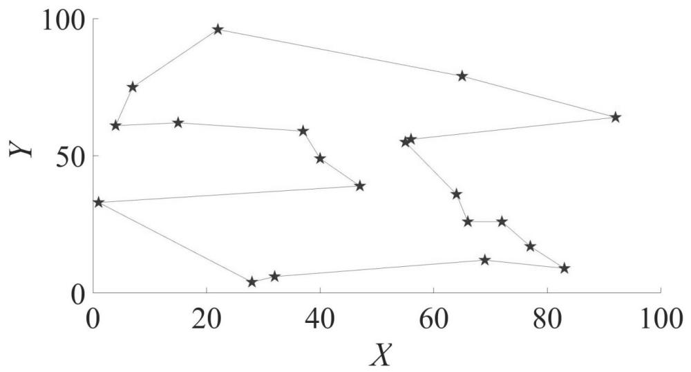
Please refer to Fig. 3, Fig. 3 is the electroluminescence path diagram when the dead pixel detection method of micro-LED of the present invention does not carry out the shortest path planning. The star in Figure 3 indicates the position of the micro-LED, the x is horizontal, the y is vertical, and the line indicates the test path. When the shortest path is not planned, the lines are interleaved, resulting in a long inspection time.
Please refer to Figure 4, and Figure 4 is the electroluminescence detection path diagram of the dead spot detection method of micro-LED of the present invention for example. In particular, after path planning, the lines between the individual micro-LEDs are no longer interlaced, which reduces the detection time.
In this embodiment, the invention can reduce the time required to move back and forth in each micro-LED in the electroluminescence detection by calculating the shortest path and then carrying out electroluminescence detection on each micro-LED according to the shortest path, so that the electroluminescence detection of each micro-LED can be completed in a relatively short time.
Optionally, in a feasible embodiment, after the preceding step S3011, the method further comprises:
step S3013, optimizing the shortest path based on the preset trajectory planning principle;
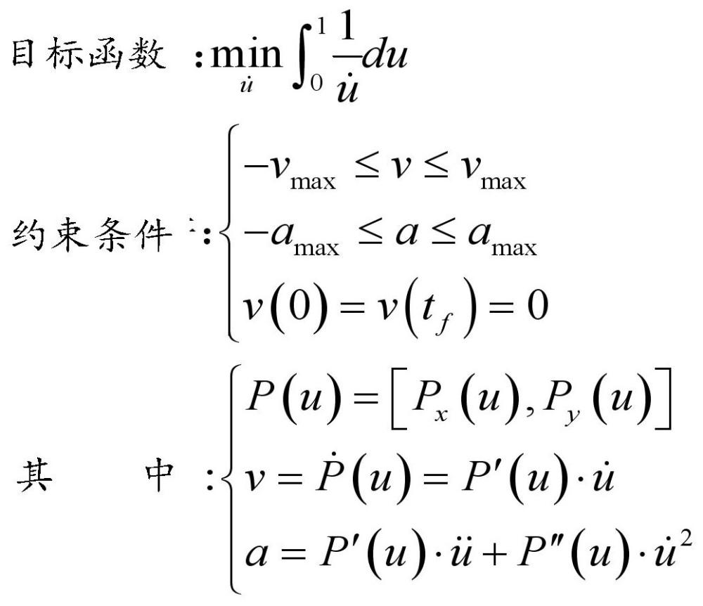
It should be noted that electroluminescence detection is a point-to-point motion, and point-to-point motion requires that the effective motion time account for as much as possible while ensuring the positioning accuracy, so as to improve the detection efficiency. For example, if you continue to refer to Figure 3, the length of the lines in Figure 3 is inconsistent, in order to reduce the time spent on the path between points, when the lines are long, it is also necessary to increase the speed of moving between points, so as to reduce the time required for movement, and thus increase the proportion of effective movement time. However, the shortest path determined by Dijkstra algorithm and Floyd algorithm can only ensure that the overall time consumption is short, but cannot guarantee that the effective movement time accounts for a large proportion. Therefore, the shortest path obtained by Dijkstra algorithm and Floyd algorithm can be optimized based on the preset trajectory planning principle to further improve the movement speed between luminescence points during electroluminescence detection.
As an example, trajectory planning principles can be:
![]()
where is the![]() parameter velocity,
![]() is the parameter acceleration,
![]() is the displacement, Vmax and
![]() are the maximum speed and maximum acceleration that the motion system can provide, v(0) and v(
![]() ) represent the velocity at 0 time and time respectively, and
![]() represent the
![]() position of the motion system when the displacement is
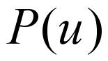
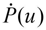
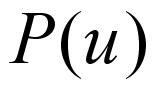
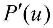
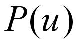
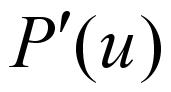
![]() time, Px represents the position in the x direction, Py represents the position in the y direction, and Px(u) represents the displacement when u, The position in the x-direction, Py(u) denotes the position in the y-direction when the displacement is u, is
![]() the differential,
![]()
![]() is
![]() the derivative, is the derivative, is the derivative.
![]()
![]()
Based on this, the above step S3012 further comprises:
step S3012-A, each micro-LED in the suspected point set and the good point set is electroluminescently detected according to the shortest path after optimization, and a second bad point set is obtained.
In the present embodiment, the invention further further increases the proportion of effective motion time through the preset trajectory planning principle, thereby improving the efficiency of dead pixel detection.
Further, based on the first embodiment and the second embodiment of the dead pixel detection method of micro-LED of the present invention, a third embodiment of the dead pixel detection method of micro-LED of the present invention is proposed.
In this embodiment, after the preceding step S30, the method further comprises:
step S200, determining the intersection of the set of good points and the set of second bad points, and determining the first quantity of micro-LEDs in the intersection;
step S300, determining the second quantity of micro-LEDs in the set of good spots, and taking the ratio of the first quantity and the second quantity as the bad pixel detection rate.
It should be noted that the bad pixel detection rate refers to the probability of detecting a bad pixel from a good spot.
In this embodiment, after obtaining a second set of bad points, the intersection of the set of good points and the set of second bad points can also be determined, and then the number of micro-LEDs in the intersection can be determined, that is, the first quantity is obtained. The number of luminous dots in the set of good dots can then be determined, i.e., the second number can be obtained, and the bad pixel detection rate can be obtained based on the ratio of the first and second quantities. As a result, the reliability of automated optical inspection and photoluminescence detection can be determined based on the numerical value of the dead pixel detection rate.
Optionally, in a feasible embodiment, the method further comprises, prior to the preceding step S10:
step S400, controlling a preset motion table to carry out a grid scanning motion through an iterative learning algorithm, wherein the motion table is fixed with the wafer.
It is understandable that when scanning and inspecting through the motion table, the wafer to be detected needs to be fixed on the motion table in advance, and the position of the wafer is adjusted by using the motion table to make the alignment direction of the light-emitting device consistent with the motion direction of the motion table.
It is worth mentioning that scanning detection needs to provide stable periodic high uniform motion. The single-pass scanning motion can generally be divided into the start-up stage, the adjustment stage, the constant scanning stage and the deceleration stage. In order to eliminate the repetitive disturbance components in the periodic scanning motion, such as the periodic fluctuation of the magnetic field, the system assembly error, the composite force switching disturbance, etc., the piecewise iterative learning algorithm can be used for feedforward compensation. The iterative learning rate is weighted to enhance the desired learning control, so as to eliminate the undesirable learning control.
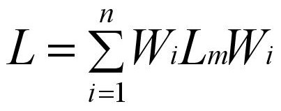
In a feasible embodiment, the expression of piecewise iterative learning control can be:
![]() ;
where L is the total control rate,![]() which is the weighted matrix of each segment learning,
![]() which is the control rate of the mth segment, and n is the total number of segments of the segment.
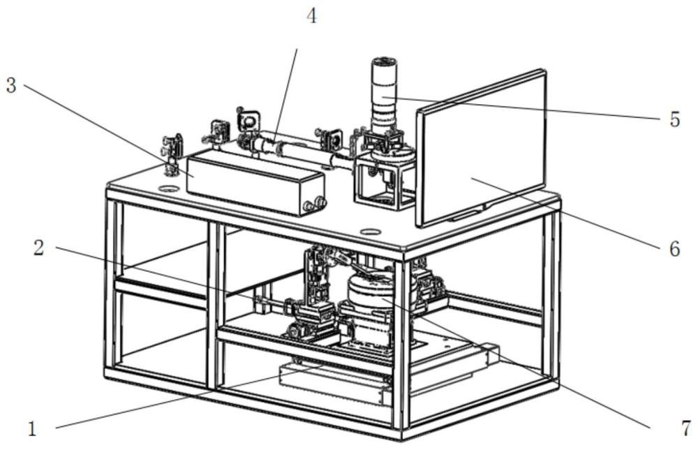
Please refer to Figure 5, and Figure 5 is the detection equipment diagram required for the bad pixel detection method of micro-LED of the present invention for an embodiment. Among them, 1 represents the motion table, 2 represents the XYZ robotic arm, 3 represents the colorimeter, 4 represents the laser optical path, 5 represents the high-speed camera, 6 represents the display screen, and 7 represents the wafer stage. The steps for the dead pixel detection of micro-LEDs by the inspection equipment shown in Figure 5 can be:
1) The wafer is placed on the upper surface of the composite drive motion stage, the light-emitting device on the wafer is imaged with a high-speed camera, and the imaging system is automatically focused by the clarity function; When the camera obtains a clear image, the wafer position is adjusted by using the motion table to make the alignment direction of the light-emitting device consistent with the motion direction of the motion table.
2) The light-emitting devices in the upper left corner of the wafer are moved into the imaging field of view through the motion table, and they are numbered as (1, 1) light-emitting devices, and the other light-emitting devices are numbered sequentially in imitation of the matrix numbering method.
3) Start the colorimeter and high-speed camera and introduce the excitation laser.
4) The motion platform performs raster scanning movements.
5) Through data analysis, the results of PL detection and AOI detection were analyzed.
6) EL detection was performed on some good points and all suspected points. The coordinates of the suspected points in the detection are sorted out, and some points are randomly selected and the coordinate positions are recorded in the good points. All location coordinates are optimized to find the optimal path. EL detection is performed based on the optimal path.
7) Analyze the EL test results.
In the present embodiment, the invention eliminates the influence of factors such as magnetic field periodic fluctuations, system assembly errors, and composite force switching disturbances on automatic luminescence detection and photoluminescence detection through iterative learning, so that the accuracy of automatic luminescence detection and photoluminescence detection of bad pixels can be improved.
In addition, the invention also proposes a dead pixel detection system of micro-LED.
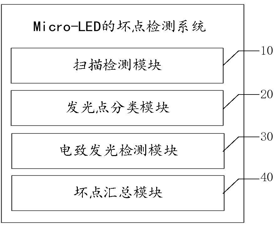
Referring to Figure 6, the dead pixel detection system of the micro-LED comprises:
the scanning detection module 10 is used for carrying out automatic optical detection on the micro-LED on the wafer to obtain the automatic optical detection result, and performing photoluminescence detection on the micro-LED on the wafer to obtain the photoluminescence detection result;
the luminescent spot classification module 20 is used for determining a collection of suspected points, a set of good points and a set of first bad points according to the automatic optical detection result and the photoluminescence detection result;
the electroluminescence detection module 30 is used for electroluminescence detection of each micro-LED in the suspected point set and the good point set, and the second bad point set is obtained;
the bad pixel aggregation module 40 is used for taking the union of the first bad pixel set and the second bad pixel set as the bad pixel detection result.
Optionally, the luminous spot classification module 20 is also used for:
based on the intersection of the good points in the automatic optical detection result and the good points in the photoluminescence detection result, a set of good points is obtained;
the first set of dead pixels is obtained based on the union of the dead pixels in the automatic optical detection result and the dead pixels in the photoluminescence detection result;
a set of suspicious points is obtained by taking a point on the wafer that does not belong to the set of good points and does not belong to the first set of bad points as a suspicious point.
Optionally, the micro-LED dead pixel detection system also includes:
the good point extraction module is used for randomly selecting the good points in the set of good points to obtain a random set of good points;
Based on this, the electroluminescence detection module 30 is also used for:
electroluminescence detection is carried out on each micro-LED in the suspected point set and the random good point set to obtain a second bad pixel set.
Optionally, the electroluminescence detection module 30 is also used for:
obtaining the coordinates corresponding to each micro-LED in the suspected point set and the random good point set, and determining the shortest path based on each coordinate;
electroluminescence detection is carried out on each micro-LED in the suspected point set and the random good point set according to the shortest path to obtain a second bad pixel set.
Optionally, the electroluminescence detection module 30 is also used for:
optimizing the shortest path based on the preset trajectory planning principle;
Based on this, the electroluminescence detection module 30 is also used for:
electroluminescence detection is carried out on each micro-LED in the suspected point set and the good point set according to the shortest path after optimization, and a second bad pixel set is obtained.
Optionally, the micro-LED dead pixel detection system also includes:
the first quantity calculation module is used for determining the intersection of the set of good points and the set of second bad points, and determining the first quantity of micro-LEDs in the intersection;
the accuracy calculation module is used for determining the second quantity of micro-LEDs in the set of good pixels, and taking the ratio of the first quantity and the second quantity as the bad pixel detection rate.
Optionally, the micro-LED dead pixel detection system also includes:
the iterative control module is used for controlling the preset motion table to carry out grid scanning motion through an iterative learning algorithm, wherein the motion table is fixed with the wafer.
Wherein, the functional implementation of each module in the dead pixel detection system of the micro-LED corresponds to each step in the embodiment of the dead pixel detection method of the micro-LED, and its functions and implementation processes are not repeated here.
In addition, the present invention also provides a dead pixel detection device of micro-LED, the dead pixel detection device of micro-LED comprises: a memory, a processor and a dead pixel detection program of micro-LED stored on described memory and can run on described processor, and the dead pixel detection program of described micro-LED is executed by described processor to realize the steps of the dead pixel detection method of micro-LED as described above.
The specific embodiment of the dead pixel detection apparatus of the present invention is basically the same as the embodiment of the dead pixel detection method of the micro-LED described above, and is not repeated herein.
In addition, the invention also provides a storage medium, on which a dead pixel detection program of micro-LED is stored, and the dead pixel detection program of micro-LED is executed by a processor to realize a step for the dead pixel detection method of micro-LED as described above.
The specific embodiments of the storage medium of the present invention are basically the same as the embodiments of the dead pixel detection method of the micro-LED described above, and are not repeated herein.
It should be noted that, for the purposes of this document, the term "including", "including" or any other variation thereof is intended to cover non-exclusive inclusions, so that a process, process, article or apparatus that includes a series of elements includes not only those elements, but also other elements that are not expressly listed, or that are inherent to such a process, method, article or apparatus. In the absence of further restrictions, an element defined by the phrase "including a ......" does not preclude the existence of other identical elements in the process, method, article or apparatus that includes that element.
The above embodiment numbers of the present application are only for description and do not represent the advantages and disadvantages of the embodiments.
Through the description of the above embodiments, those skilled in the art can clearly understand that the above embodiment method can be realized by means of software plus the necessary general hardware platform, and of course it can also be achieved by hardware, but in many cases the former is a better embodiment. Based on this understanding, the essence of the technical solution of the present application or the part that contributes to the prior art may be embodied in the form of a software product that is stored in a storage medium (such as ROM/RAM, a disk disk, an optical disc) and comprises a plurality of instructions to enable a terminal device (which may be a vehicle-mounted computer, a smart phone, a computer, or a server, etc.) to execute the methods described in each embodiment of the present application.
The above is only a preferred embodiment of the present application, and does not limit the scope of the patent of the present application, and all equivalent structural or equivalent process transformations made by using the contents of the description and drawings of the present application, or directly or indirectly used in other related technical fields, are similarly included in the scope of patent protection of the present application.















 400-4929-0909
 contact@catarc.com.cn

